
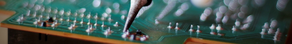
Question: We install D-Paks on a number of boards (8.3.14 in IPC-A-610). These parts have a tendency to float during reflow. We have done quite a bit of process work to minimize the floating, but parts do still occasionally float and are...
Question: We install D-Paks on a number of boards (8.3.14 in IPC-A-610). These parts have a tendency to float during reflow. We have done quite a bit of process work to minimize the floating, but parts do still occasionally float and are...