
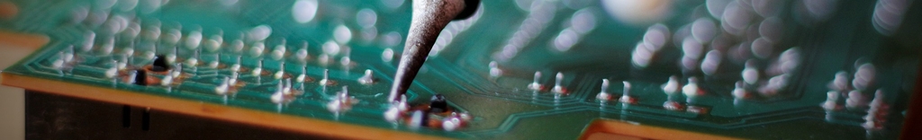
Question: We are having a discussion about whether or not solder can touch a component body; in particular, we have a plastic SMT component where the solder has wicked up to the body on the legs. Sections are shown below. Is this condition acceptable under any circumstances, or is it always a reject in all three classes?
Question: We are having a discussion about whether or not solder can touch a component body; in particular, we have a plastic SMT component where the solder has wicked up to the body on the legs. Sections are shown below. Is this condition acceptable under any circumstances, or is it always a reject in all three classes?
Answer: Based upon the requirements of IPC-A-610, solder is not allowed to touch a component body. For through hole components see Section 7.3.5.7 – Supported Holes, Solder Conditions – Touching Through Hole Component Body. For surface mount components see Section – 8.3.5.5 Flat Gull Wing Leads p Maximum Heel Fillet Height (E).
The overall intent is that the solder can climb up the lead but not touch the body. When solder touches the body of a component, be it either PTH or SMT components, there is a possibility that it can destroy the seal where the lead enters the component body and cause issues in the component by allowing moisture to enter resulting in latent failures, basically failures in the field.
The same criteria applies to surface mount components as is stated in the notes beneath Tables 8-5 and 8-6 in the surface mount section of IPC-A-610. The reason being is that if the solder does touch the body it will reduce or eliminate the stress relief characteristic of the leads, which can cause physical component damage and failures, either detected in test or latent in the field.
Now, all that being said, the question arises as to how this condition actually occurred. Were the components received this way, i.e. did this condition occur from tinning of the leads? In this case, the argument may be made that this is not a reject condition. In the strictest interpretation of the 610 standard, these components would still be rejected and dispositioned. What this means is that after identifying the defect, you have the responsibility to disposition the components to be used as-is, reworked, or scrapped. This decision is also dependent on the application. The more reliability requirements in the final product, the less likely the components use.
If this condition occurred during a wave or reflow soldering process, then this points to underlying process issues. With wave soldering, if there is excessive solder flow up through the holes, this may indicate the possibility that the board is traveling too slowly in the process. In reflow, excessive solder paste may be applied during the stenciling process. Regardless, these process indicators should be reviewed and addressed.