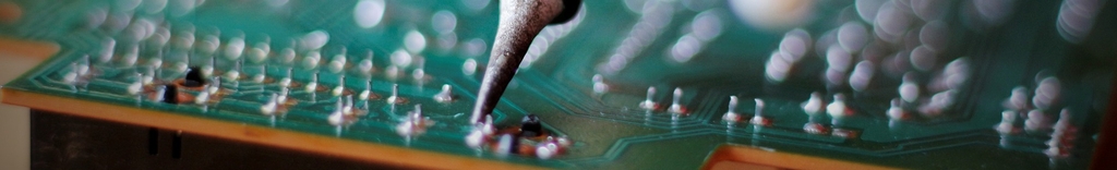
Gold and electronics have had a partnership in products and components for many years. The initial reasoning behind the application of gold to printed circuit boards was to make them more susceptible to the application of wire bonding and for corrosion protection. At the time, the gold layer was applied very thickly, typically 50 mils which created numerous soldering quality issues when attaching components to assemblies. It was found that the gold would go into solution and create a thick gold intermetallic condition creating fracture condition in solder joints.
The military and industrial soldering specifications typically required the removal of gold plating from components which were to be soldered onto printed circuit boards to prevent gold intermetallic from forming and from cracking of the solder joints. Today we must ask ourselves, where this reasoning came from and what has happened to make it so.
More to the point there have been changes regarding gold plating and its removal with the introduction of the new J-STD-001 “Requirements for Soldered Electrical and Electronic Assemblies” Revision F. These changes from Revision “E” to Revision “F” have created some subtle requirements in the electronics manufacturing process, which you should be aware of.
J-STD-001 Revision “E” stated:
4.5.1 Gold Removal
Gold shall be removed:
- a. From at least 95% of the surfaces to be soldered of the through-hole component leads with 2.54 μm [100 μin] or more of gold thickness.
- b. From 95% of all surfaces to be soldered of surface mount components regardless of gold thickness.
- c. From the surfaces to be soldered of solder terminals plated with 2.54 μm [100 μin] or more of gold thickness.
A double tinning process or dynamic solder wave may be used for gold removal prior to mounting the component on the assembly.
J STD-001 Revision “F” now states: (note that the new wording/changes are highlighted below)
4.5.1 Gold Removal
Gold removal is performed to reduce the risk of failure associated with embrittled solder. Gold embrittlement is not a visually inspectable anomaly. In cases where analysis has determined there is a gold embrittlement condition, the gold embrittlement shall be considered a defect, see IPC-HDBK-001 or IPC-AJ-820 handbook for guidance. Except as noted above, gold shall be removed:
- a. From at least 95% of the surfaces to be soldered of the through-hole component leads with >2.54 μm [100 μin] gold thickness and all through-hole leads that will be hand soldered regardless of gold thickness.
- b. From 95% of all surfaces to be soldered of surface mount components regardless of gold thickness.
- c. From the surfaces to be soldered of solder terminals plated with >2.54 μm [100 μin] gold thickness and from all solder cup terminals, regardless of gold thickness.
A double tinning process or dynamic solder wave may be used for gold removal prior to mounting the component on the assembly.
Note: Gold embrittled solder connections can occur regardless of gold thickness when solder volume is low or the soldering process dwell time is not sufficient to allow the gold to dissolve throughout the entire solder joint.
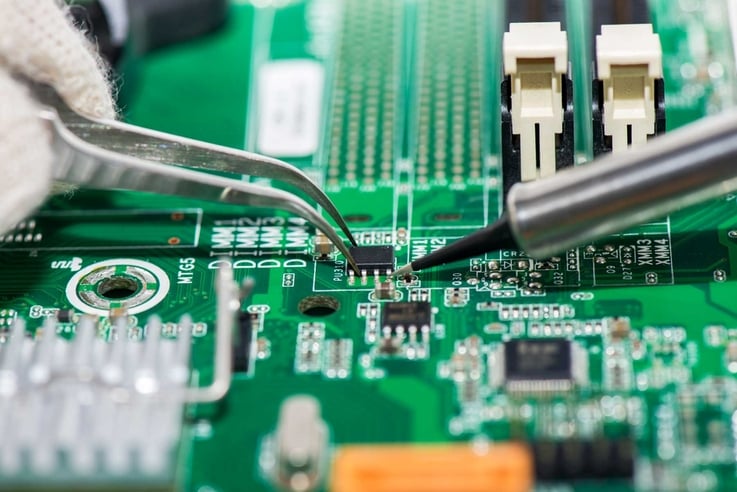
The emphasize of these changes are due to problems in the field with gold embrittlement, simply stating that all plated through hole components that are to be hand soldered must be tinned regardless of the thickness of the plating. This same condition also applies to gold cup terminals, i.e. all the gold must be removed from within the cups regardless of gold thickness. These are the two most important changes occurring as we transition to the latest commercial revision.
The concern of course is gold embrittlement as stated in the last NOTE in Revision “F” above. Gold embrittlement can occur regardless of gold thickness when the solder volume is too low or the soldering process dwell time is not sufficient to allow the gold to dissolve throughout the entire solder joint. Because of this, the gold has to be completely removed so that the solder makes the electromechanical and/or metallurgical bond to the subsurface beneath the gold, which in most cases is Nickel.
As stated in a article by Eric Bastow of Indium Corporation: Intermetallics in Soldering
“Keep in mind that dissolution, the phenomenon of a solid dissolving into a liquid, is affected by both time and temperature. Generally speaking, more time and more temperature allows for more dissolution and, hence, more intermetallic formation. “
You can read more of his article here:
http://www.indium.com/blog/intermetallics-in-soldering.php
There are many articles and papers that have been presented on the whole gold plating issue since its introduction into the manufacturing process on printed circuit boards and in the plating on the component leads. Although gold is a noble metal, the methodology for its application, be it electroplating or immersion plating, gold will still go into a molten tin/lead or tin solder solution. The percentage of gold within the solution has to be analyzed with the current maximum gold percentage by weight being 3 wt. %. At higher percentages, the failure rate increases from the intermetallic and gold dendrites within the solder itself. Once the solder has solidified, those gold dendrites can act as stress risers and can initiate cracks within the solder joint.
See IPC Listserv Technet for more information on gold, the gold plating processes and the reliability issues created by gold intermetallics. Additionally information can also be researched on the Internet related to this topic.