
Why All PCB Designers Should Receive CID/CID+ Certification
Read More
Posted on 29st August, 2023 by EPTAC
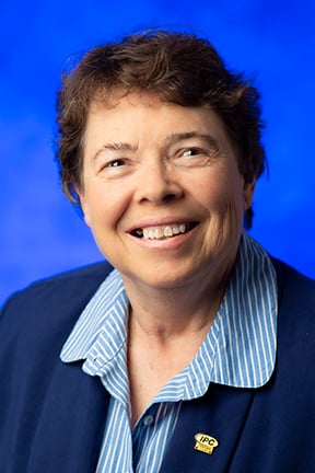
This is the fourth article in our "EPTAC Team Spotlight" series. Today, we're presenting an interview with Cherie Litson, a dedicated PCB design instructor. In this discussion, Cherie shares her entry into the PCB design world, her interactions with key figures in the industry, and her role as an instructor at EPTAC. We'll also touch on the challenges she faced in her career and get her views on the future of PCB design. Join us as we learn more about Cherie's professional journey and her experiences with EPTAC.
I took the CID in Seattle in 1998. The CID was very new at that time, and since I had barely passed, I was determined to learn more about this field I thought I knew. Deiter Bergman, the instructor, recommended that we all attend PCB West. That’s when I met Gary Ferrari and Mary Sugden. It was the first time I had ever been to a convention based on the principles and industry surrounding PCB Design. I was surprised! I discovered that there were standards and guidelines written for every aspect of the PCB development process. I got books, standards, business cards, and promised to follow up with many of those I met that week.
Unfortunately, when I returned home, a doctor's appointment changed my intentions for a couple of years. I had ovarian cancer and went into surgery shortly after returning. It didn’t stop me completely, though. I started a Designer Council (DC) group in the Seattle area and began networking with many great people. One of them was a sales representative from Prototron Circuits. The entire staff at Prototron was a huge support to me as a designer, helping build a network for the Designer Council group, and throughout my recovery from cancer.
It didn’t stop me completely, though. I started a Designer Council (DC) group in the Seattle area and began networking with many great people.
Being a part of the Designer Council, attending PCB West, and the west coast IPC APEX were foundational experiences. As president of the Cascade Designers Council, I had amazing opportunities to meet many experts in the PCB design & development industry. We organized workshops and presentations on Fabrication, Materials, Assembly, design techniques, engineering considerations, and more. We conducted tours and held meetings with the SMTA and the Portland PNW Designer Chapter. Our council invited representatives from all major software companies to showcase their software. We also sponsored numerous CID & CID+ courses during those years. And yes, I achieved the “Top Dog” score on my CID+ exam.
As president of the Cascade Designers Council, I had amazing opportunities to meet many experts in the PCB design & development industry.
Between 2004 and 2005, I joined the National Designer Council Board. It was then that I became an Instructor for the CID, and later, the CID+. Over time, I served on the Executive DC Board and contributed to the rewrite of the CID & CID+ course and exam in 2016, a collaborative effort involving representatives globally.
As the oldest of 9 children, I learned early on how to take charge and keep people’s attention. This has served me well as an instructor, regardless of what I teach. I’ve come to realize that it isn’t the subject or medium you teach that matters most, but rather the engagement created by the instructor. When you think of instructors who've made a difference in your life, it's often because they genuinely engaged you in the subject.
When you think of instructors who've made a difference in your life, it's often because they genuinely engaged you in the subject.
With the CID, it took me some time to feel comfortable teaching it. There's always so much to learn in this field. Every time I teach, I'm reminded of how much more there is to discover about this industry. And in every class, I find that I learn something new from my students! I love that and make a point to acknowledge it.
I read, talk, engage with others, attend conferences & classes, serve on college advisory boards, and I teach. I teach a Basic Electronics class at one of our community colleges. I get to pick the weeks, days, and time I want to teach, so it’s a sweet gig! I had to develop the course from an outline, write a study guide, and come up with experiments for hands-on training. Often, I have adult students who know a lot about electronic theory but have never built or tested a circuit. It’s a blast to see them truly "get" the concepts.
This approach extends to my CID & CID+ trainings as well. I use examples from products I've either torn apart or built myself to show. I have a robust online presentation setup that lets me show them actual objects. In-person classes are great because students can touch these objects, like feeling how much 1 oz of copper weighs or what prepreg feels like. They get to see the actual size of the components and traces they're designing, not just on the computer screen.
People in our field need both hands-on experiences and theoretical knowledge. Designers are at the "HUB" of product development. EVERYTHING we do affects everyone else.
Designers are at the “HUB” of product development. EVERYTHING we do has an effect on everyone else.
This subject has been an area that I am truly concerned about. I’ve been writing some articles about this for 007 PCB Design and talking with some of the companies that are investing in techniques to address some of the issues. Here’s a summary of what I see:
I’ve found through the many years I’ve been doing design that very little is “impossible” to accomplish. It just might cost more for a while or take a little longer to get done. Eventually, we’ll find a way to make this the “normal” way to build products. Then we’ll find new challenges!
I’ve found through the many years I’ve been doing design that very little is “impossible” to accomplish. It just might cost more for a while or take a little longer to get done.
Gary Ferrari first introduced me to the EPTAC family. I met many of them at the IPC Apex in San Diego, CA. When IPC decided to move the management and promotion of their trainings to the companies that were conducting these trainings, Gary suggested we keep all the CID & CID+ instructors under one training group to maintain program consistency. This would ensure that we upheld the same training principles everywhere.
EPTAC has been a huge supporter of the Design Industry, as well as the fabrication and assembly industry. I have enjoyed the absolute support from the staff. They keep me informed of any changes, take care of any travel arrangements we need, offer extra training opportunities to all the instructors, and keep us as a team even though we are many miles apart.
They keep us as a team even though we are many miles apart.
One of the most memorable moments in my career as part of the Designer Council and EPTAC was bringing my mom to an IPC APEX in Las Vegas to see me receive an award from IPC for contributing to the CID & CID+ program. She was very impressed.
The greatest success any instructor can experience is when a student becomes a peer. The first time was when I certified Stephen Chaves as both a CID and a CID+ instructor. The second time was when I certified Dave Seymour as a CID instructor. Every time I attend a conference, I see many former students stepping up to take on the roles of presenters, trainers, and leaders in PCB Design.
The greatest success any instructor can experience is when a student becomes a peer.
Besides the wonderful support I receive from the staff at EPTAC, they have provided me with opportunities to grow, learn, and network with people across the world. That's something very few companies offer. I am humbled by the opportunity to work with them and am continually inspired to expand my own skills.
I am humbled by the opportunity to work with them and am continually inspired to expand my own skills.
EPTAC is an internationally recognized leader in solder training and IPC certification, providing professionals with the skills to accelerate their careers and businesses and the talent to succeed. For over 35 years, EPTAC has been helping corporations increase quality standards, improve productivity, and maximize profits. With 24 locations in North America, EPTAC continues to expand its offerings and exceptional instructional staff to provide easy access to knowledge and skill-based programs when and where the industry demands it. Access our scheduled programs through our website or schedule your own corporate on-site training. For more information, call 800.643.7822 or contact us.