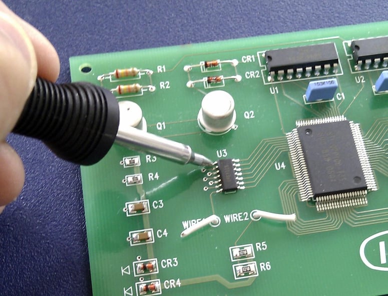
Being a crucial component of all electronics, top technologies around the world rely on precise PCB design. However, despite its intricate nature, the design process can be prone to errors. These mistakes can lead to production delays due to necessary board reworks. To prevent functionality errors, it's essential to be aware of three common PCB mistakes to watch out for.
Landing Patterns
While most PCB design software comes equipped with libraries containing common electrical components, their corresponding schematic symbols, and landing patterns, there are instances where designers may need to manually draw them. Given the potential for errors at less than half a millimeter, engineers must pay close attention to ensure the correct spacing between pads. Any mistakes at this stage could lead to difficulties in soldering or even render it impossible, ultimately resulting in costly reworks and delays.
Using Blind/Buried Vias
In today's tech-savvy market, the rise of IoT devices has highlighted the impact of compact, smaller products. When designing PCBs for these smaller devices, engineers often turn to blind and buried vias to reduce the board's size and connect internal and external layers. While these vias are effective in shrinking the PCB footprint, they can complicate routing space as more are added, potentially making some boards costly and challenging to manufacture.
Trace Width
To maintain a small and compact board size, engineers strive to keep traces as narrow as possible for optimal functionality. The process of determining PCB trace width can be challenging due to various factors, so it is crucial to have a comprehensive understanding of the required milliamps. In most scenarios, relying solely on the minimum width may not be sufficient. We suggest utilizing a width calculator to accurately determine the appropriate thickness and ensure precise design outcomes.
Identifying these errors early on can help prevent any disruptions in production and ensure your PCB functions effectively. To excel in electronics manufacturing and create top-notch PCBs, consider reaching out to the experts at EPTAC and enrolling in a PCB designer course today.

About EPTAC
EPTAC is an internationally recognized leader in solder training and IPC certification, providing professionals with the skills to accelerate their careers and businesses and the talent to succeed. For over 35 years, EPTAC has been helping corporations increase quality standards, improve productivity, and maximize profits.
With 24 locations in North America, EPTAC continues to expand its offerings and exceptional instructional staff to provide easy access to knowledge and skill-based programs when and where the industry demands it. Access our scheduled programs through our website or schedule your own corporate on-site training. For more information, call 800.643.7822 or contact us.